

What are the P-Type Semiconductors
What is Mean by a Semiconductor
(what are the P-Type semiconductor)
Semiconductors are the materials which conductivity is between conductor and insulator. It can be compound which includes gallium arsenide or it can be pure elements which includes germanium and silicon. It is classified into two types which are intrinsic and extrinsic. Intrinsic semiconductors are pure semiconductor materials which include germanium and silicon while extrinsic semiconductors are the materials which are doped with impurities to change their properties. It is used in electronic circuit fabrication, laser diodes etc.
What are the Semiconductor materials
Semiconductor materialsinclude.
- Silicon: it is the semiconductor materials which is mostly used in the electronics industries.
- Germanium: it is the semiconductor material which is used in the construction of transistors and diodes.
- Gallium arsenide: Gallium arsenide electron mobility is higher than silicon, which allows faster operation. It has a wider band gap which is useful in the operation of power equipment in high temperatures. It gives low noise to power equipment at room temperature.
What are the P-Type Semiconductors
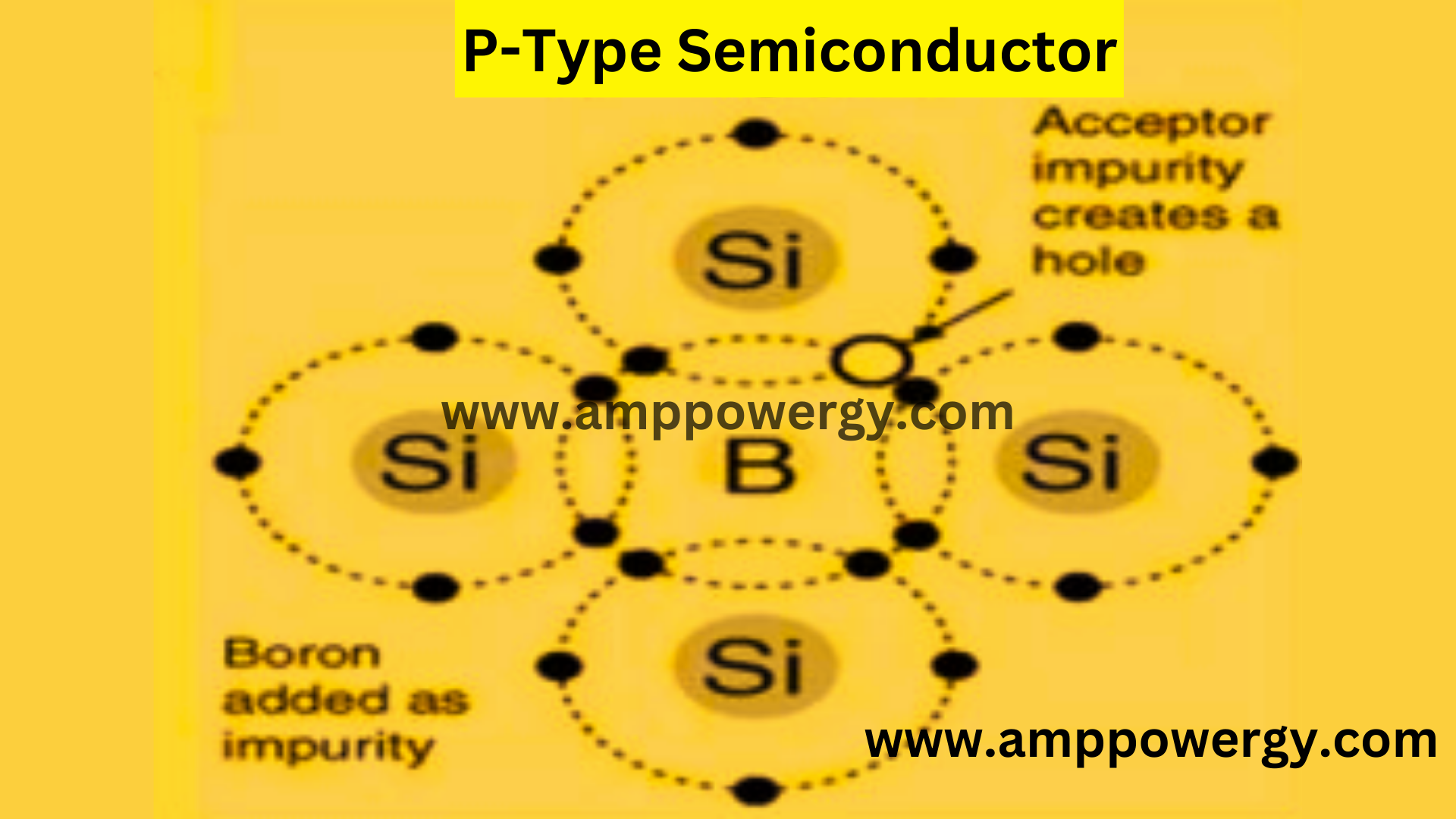
P type semiconductor is the type of semiconductor. When an impurity of trivalent is added to the intrinsic or pure semiconductor, then it is known as p type semiconductor. The trivalent impurity is boron, aluminum etc. which is added to the intrinsic semiconductor and the intrinsic or pure semiconductor is silicon or germanium. The trivalent impurities like gallium (Ga), boron (B), indium (In) etc. are called the accepter impurity.
Usually, semiconductors are materials that do not conduct electricity because they do not have free electron, but they are not highly resistive. Metalloids such as silicon (Si), germanium (Ge), Arsenic (As) and a few more elements are commonly used for the main body of semiconductors. These elements fall in between insulator and conductor therefore it is called semiconductor. To flow electric current in the materials there must be an electron hole in the materials to move electron into. In p type semiconductor there are more holes in the electron. And this allows the current to flow in the materials from hole to hole, but this current is a one direction.
Semiconductors are mostly made from silicon; silicon is the atom which has four electrons in its outer most shell. Noe to make p type semiconductor extra materials are added to the silicon that extra materials are boron or aluminum, and these materials have three electrons in their outer most shell, when the extra materials replace silicon, its leave some holes.
P type semiconductor accepts the electron, so they are doped with accepter, while N type semiconductor is doped with doner because they donate electron. The PN junction relies on the diffusion of the electron from n type to p-type semiconductor.
What is Mean by Doping
Actually, doping is the process of adding impurities to the semiconductor materials to change its ability. The two most used materials are silicon. Silicon can be doped with boron. Boron has 3 electrons in its outer most shell. Silicon can also be doped with phosphorus (phosphorus has 5 electrons in its outer most shell). The other materials ae indium which has 3 electrons in its valance shell, aluminum, antimony which has 5 electrons in its outer most shell.
Dopant is added to the structure of the semiconductor materials. The number of valance electron decide the type of doping. The element which has 3 valance electron is used for p type semiconductor materials and the element which has 5 electrons in its outer most shell is used for n type of semiconductor materials.
Doping in a p type of semiconductor
Doping is the prosses od adding impurities to semiconductor to change its properties. In the case of p type semiconductors, trivalent impurity is added to them. The trivalent impurity includes indium and boron. This trivalent Impurity is added to the intrinsic semiconductor. Intrinsic semiconductors include silicon and germanium. This impurity is added to the crystal structure, but one electron is missing which makes a hole in the valence band and this hole can be filled by an electron from the conduction band.
In a result net positive charges create, and the semiconductor materials becomes p type semiconductor materials.
Manufacture of P-Type Semiconductor
P type semiconductors are made from doping like doped pure semiconductor materials, but the amount of impurity to be added to the semiconductors is very small as compared to the semiconductor. In p type semiconductor the amount of hole is greater than the thermally generated electrons’
Now suppose the impure trivalent atom are doped in silicon. Now after doping each trivalent atom make three covalent bonds with the neighbor silicon atom but the trivalent atom does not have fourth electron to make bond, this absence create a hole which have positive charge and this hole i.e., increase the conductivity of the semiconductor, there are thousands of impure atoms. Each impure atom donates one hole as a result the amount of positive charge increases and the conductive of semiconductor increases even at room temperature.
What are the Properties of P-Type Semiconductor
- P type of semiconductor is formed by doping a trivalent atom in pure semiconductor crystal.
- The majority carriers in the p type semiconductor are holes.
- The minority carrier is free electron.
Example of P-Type Semiconductor
- Boron doped silicon.
- Aluminum doped silicon
- Aluminum doped germanium
- Boron doped germanium.
These all are the example of p type semiconductor, other semiconductor with trivalent impurities are p type semiconductor.
Energy Band Diagram for the P-Type Semiconductor
P type semiconductor materials are doped with trivalent impurities. Many holes are formed in the p type semiconductor materials so, the majority carriers are holes, and the minority carriers are electrons in the p type semiconductor. Because the majority carriers are hole, p type semiconductor are referred to as a positive type.
The fermi level of the p type semiconductor is near to valence band and away from the conduction band. When impurity is added to the materials many holes are formed in the valence band but there is thermal excitation in the conduction band, so the same amount of electron is also present in the conduction band. Due to the large number of holes as compared to electron the materials became p type of semiconductor.
As the diagram shows there are less electrons in the conduction band as compared to holes in the valence band.

Uses of P-Type Semiconductor
Pure semiconductor is a very poor conductor at room temperature, but it can be made highly conductive semiconductor with doping with the impure atoms. p type semiconductor is high conductivity at room temperature. Its uses include designing transistor, diodes, BJTs, MOSFETs, solar cells etc.
Comparision
| Basic of comparison | P type semiconductor | N type semiconductor |
| definition | It is created by adding trivalent impurities in intrinsic semiconductor | It is created by adding pentavalent impurity in intrinsic semiconductor |
| Types of impurity added | Trivalent impurities are added to it which include: Aluminum, gallium and indium | pentavalent impurities are added to it which include: Aluminum, gallium and indium |
| Majority charge carries | Majority charge carriers is holes | The majority of charge carriers in N type semiconductor are electrons. |
| Density of charge carriers | Density of charge carriers is low in p type semiconductor | Density of charge carriers is high in N type semiconductors. |
| Fermi level | Fermi level is closed ton valence bond in p type semiconductor. | Fermi level is closed to conduction bond in N type semiconductor. |
Application of p type semiconductor
- Diodes: p type semiconductor are used in the creation of p-n junction of the diode. Which is used in rectifier, voltage regulation and signal detectors.
- Transistors: it is used in the base region of the BJTs (bipolar junction transistor). Which is used to control current.
- Solar cells: p types of semiconductors which includes gallium arsenide are used in the building of solar cells.
Advantage of P-Type Semiconductor
- Lower power loss: lower power loss occurs in the p type of semiconductor as compared to n type of semiconductor.
- Smaller size and weight: its weight is less, and size is small compared to other semiconductors.
- Higher resistivity: p type semiconductor resistivity is high as compared to conductor but lesser than the insulator.
- Suitable for solar cells: it is very suitable for solar cell that’s gallium arsenide is used in the building of solar cells.
Disadvantage of P-Type Semiconductor
- Temperature sensitivity: it is very sensitive to the temperature, when changes come in temperature it affects the p type semiconductors which can affect its performance.
- Lower conductivity: their conductivity is lower compared to n type of semiconductor.
Frequently asked question
Q1: what is p type of semiconductor?
Ans: it is a semiconductor which is doped with the impurity which includes boron or gallium. When n type and p types of semiconductors are connected it forms a p-n junction and this is the basis for many electronic devices.
Q1: what are the advantages of p type semiconductor materials?
Ans: the main advantage of p type semiconductor includes,
- Lower power loss.
- Smaller size and less weight.
- High resistivity than conductor.
- Lesser resistivity than insulator.
- Usage in solar cells
Q1: what are the disadvantages of p type semiconductor materials?
Ans: the disadvantage of p type semiconductor includes;
- Sensitive to temperature.
- Lower conductivity as compared to n type of semiconductor.
See Also:
2 thoughts on “P-Type Semiconductor, Properties, Application, Advantage | Disadvantage”