

In this article you will know about N Type Semiconductors, its uses, how it is created, energy band diagram and conduction through N Type semiconductors.
What is Mean by Semiconductor
Semiconductors are the materials which are the properties of both conductor and insulator. There are two types of semiconductor materials, intrinsic and extrinsic. The intrinsic ones are the semiconductor materials with no doping and therefore it is called pure semiconductor, on the other hand the extrinsic semiconductor are the semiconductor materials with doping that as impurity atom will be added to it. Based on the impurity atom it is divided into two types N type and p type semiconductor materials.
What is Mean by N-Type Semiconductor
A n type semiconductor is the type of extrinsic semiconductor which is doped with the pentavalent impurity. Pentavalent impurity has five electrons in its outer most shell. This impurity is added to the N-Type semiconductor to increase the number of electrons in the atom, so it will increase conductivity of the materials.
Doping in N-Type Semiconductors
N type semiconductors are doped with pentavalent impurity. pentavalent impurity has five electrons in its valance shell. Phosphorus (P), Arsenic (As), Antimony (SB) these three impurities are examples of pentavalent impurity. This impurity is added in a very little amount in the n type semiconductor, that is this impurity does not disturb the crystal own structure. The pentavalent impurity creates covenant bonds with silicon atom and the one electron in pentavalent impurity remains unbounded. Every pentavalent impurity atom donates one electron to the N type semiconductor materials, so it is called donor impurity. So, electrons are in greater amount in n type semiconductor.
Example on N-Type Semiconductors
Intrinsic semiconductors like silicon (Si) which have 15 electrons with the configuration of 2,8,4 and germanium which have 32 electrons with the configuration of 2,8,18,4. Now these atoms require 8 electrons in its valence shell to be stable, so intrinsic semiconductor atoms share their electron to form covenant bond and balance their atomic structure.
Manufacturing of N type semiconductor
N type semiconductor is created by doping, pure silicon crystal is doped with the pentavalent impurity like antimony (Sb), silicon atom has four electrons in its valence shell each silicon atom makes covenant bond with the pentavalent impurity,
Antimony (Sb) has five electrons in its valence shell, four electron makes bond with four silicon atom and the fifth one remains unbonded, this fifth electron is loosely bonded with its parent antimony atom and when external voltage or head is applied to the atom its Easly break its bond and become free and takes contribution in conduction. In n types of semiconductors materials, the majority carriers are free electron.
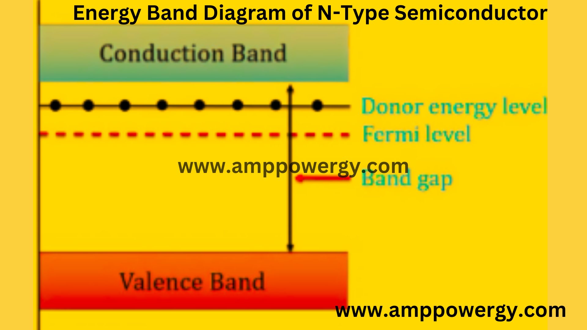
What is Energy diagram of N-Type Semiconductor
In the energy band diagram there are two bands, one is the valence band, and one is the conduction band, the electron which is in the valence band are the electrons which are the valence band of its parent atom and are bonded to the parent atom. And the electrons which are in the conduction band are the electrons which take part in the conduction, and there is the energy gap between the valence band and conduction band is called forbidden band or band gap.
In n type semiconductor, the pentavalent has the most loosely bonded electrons. As voltage is applied to it, the bond between the electron and its valence shell breaks and takes part in the conduction. These electrons are depicted in the conduction band. When voltage is applied these electrons cross the forbidden band and jump to the conduction band a very a smaller number of holes are formed in the valence band as the electron jumps to the conduction band
Conduction through N Type Semiconductor
The conduction in n type semiconductor is caused by free electron. And these free electrons are donated by pentavalent impurity, as the voltage applied to the lattice structure means to the pentavalent atom the electron gains energy the electrons break its covenant bond and jumps to the conduction band and leave a hole on its place.
The hole has a positive charge which attracts more electrons; thus, the n type semiconductor has two types of carriers, electron and hole. The amount of electron is more than the hole, so the majority carriers are electron in the n type semiconductor, the current in the n type semiconductor which caused by electrons are called as majority carriers current and the current which is caused by hole is called as minority carrier current.
When an electron jumps to the conduction band and leaves a hole the other electron comes to this hole, thus electron and hole move in opposite direction. The holes are attracted toward the positive terminal of the battery and the electrons are attracted toward the negative terminals of the battery.
The majority carriers in the n type semiconductor are electron due to this n type semiconductor are used to manufacture the semiconductor device like PN junction diode, BJTs AND FETs.
Comparision of N type and P Type Semiconductors
| Basic of comparison | P type semiconductor | N type semiconductor |
| definition | It is created by adding trivalent impurities in intrinsic semiconductor. | It is created by adding pentavalent impurity in intrinsic semiconductor. |
| Types of impurity added | Trivalent impurities are added to it which include: Aluminum, gallium and indium | pentavalent impurities are added to it which include: Aluminum, gallium and indium |
| Majority charge carries. | Majority charge carriers is holes. | The majority of charge carriers in N type semiconductor are electrons. |
| Density of charge carriers | Density of charge carriers is low in p type semiconductor. | Density of charge carriers is high in N type semiconductors. |
| Fermi level | Fermi level is closed ton valence bond in p type semiconductor. | Fermi level is closed to conduction bond in N type semiconductor. |
Application of N type semiconductor
N type semiconductor have different application in electronics which are listed below
- Transistor: it is used to make the emitter and collector region of BJTs. It is also used to make the source and drain region of MOSFETs.
- Solar cell: it is used in solar cells construction. It is also used as a bottom layer of solar cells which absorb light and produce electrons.
- Light emitting diodes: it is used as a n type layer in the p-n junction of the diode. It produces light when electric current passes through them. N type semiconductor used in the making of light emitting diodes (LEDs).
- Integrated circuit: it is used in the building of ICs. It is also used as a n type layer of p-n junction.
Advantage of n type semiconductor
- electron mobility in n type semiconductor is higher than the p type semiconductor, which makes them usable in many electronics applications.
- Because of high electron mobility in the n type of semiconductor it is more conductive than p type semiconductor and it is widely used in many applications.
- It is used in the making of solar cells.
- It is used in the production of LEDs.
Disadvantage n type semiconductor
- It can damage light more easily than p type semiconductor.
- It is costly than p type semiconductor.
- It is more sensitive to temperature changes than p type semiconductor.
Frequently Asked Question FAQs
Q1: What is an n type of semiconductor?
Ans: n type semiconductor is intrinsic semiconductor which is doped by pentavalent impurity. Pentavalent impurity has 5 electrons in its outer most shell. Four electrons in them create covalent bonds while one electron remains unbounded. Pentavalent impurity is added in semiconductors to increase the number of electrons in the atom for better conduction.
Q2: What is the difference between N type and p type semiconductor?
Ans: the main difference between p and n type semiconductor is. In p type semiconductor trivalent impurity is added and in n type semiconductor pentavalent impurity is added. In n type semiconductor the majority carriers are electrons while in p type semiconductor the majority carriers are hole and the minority carriers in p type semiconductor are electrons. The fermi level of p type semiconductor is very close to valance band while the fermi level of n type semiconductor is close to conduction band.
Q3: what are the applications of N type semiconductor?
Ans: n type semiconductor is used in the wide range of application in the field of application which is listed below.
- Transistors
- Solar cells
- LEDs
- ICs
Q4: what are the advantages of N type semiconductors?
Ans: advantage of the N type semiconductor includes:
- Electron mobility is high in n type semiconductor.
- Electron density is high in n type semiconductor.
- n type semiconductor is more conductive than p type semiconductor.
- n type semiconductor is used in many applications such as solar cells, ICs and LEDs.
Q5: what are the disadvantages of n type semiconductor?
Ans: the disadvantage of n type semiconductor includes:
- More expensive than p type semiconductor.
- Damage from light easily.
- More sensitive to temperature than p type semiconductor.
watch video about N type semiconductor:
Video Link
See Also:
- p type semiconductor
- current divider rule
- voltage divider rule
- best battery tester
- current and voltage
- nuclear plants
- largest hydropower plant
- ohm law
- types of insulators
That all about N type Semiconductors
Thanks For coming ampowergy.com/
6 thoughts on “N Type Semiconductor, its Application, Advantage and Disadvantage”